Know The Theory of Partial Inductance to Control Emissions
By Glen Dash, Ampyx LLC, GlenDash at alum.mit.edu
Copyright 1999,
2005 Ampyx LLC
The theory of partial
inductance is a powerful tool for understanding why digital circuits radiate
and in designing strategies to mitigate this radiation. In fact, it can be fairly said that nothing
is more central to understanding EMI phenomena than understanding of the theory
of partial inductance.
We will begin with the
classic definition of inductance. Inductance
is defined as the ratio of magnetic flux that passes through a surface bounded
by a closed loop to the magnitude of the current generating that flux. Mathematically:

Where:
L =
Inductance in Henries
y = Magnetic flux through a surface bounded by a closed
loop
I =
Current generating y in Amps
The “surface bounded by a
closed path” could be any surface, but often what is meant is the area enclosed
by a planar wire loop. Strictly
speaking, inductance is only defined for closed paths, that is complete
loops. However, physicists have found
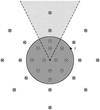
it useful to assign a partial inductance to portions of a loop. The concept is illustrated in Figure 1. Current flowing in a loop creates a magnetic
field passing through a surface bounded by the loop itself. That allows calculation of the loop’s
inductance from Equation 1. In order to
assign a partial inductance to a portion of the loop, we can divide the loop into
segments and, with a fair degree of physical accuracy, state that each segment
has its own partial inductance. Adding
the partial inductances of the segments together equals the total
inductance.

Figure 1: A loop of wire carrying current I has
an inductance equal to the ratio of the magnetic flux through the loop divided
by the current. Here, lines of flux are
shown either as moving into the plane of the page (cross within a circle) or
out of it (dot within a circle). A
portion of the loop can be assigned a partial inductance by calculating the flux
through the pie shaped area outside the loop.
To assign a partial
inductance to a segment of a loop, the segment is identified and then an area,
either inside or outside the loop, is assigned as shown in Figure 1. Measuring the total flux through either of
these areas and dividing it by the current in the segment yields the partial
inductance. Usually the area outside
the loop is used.

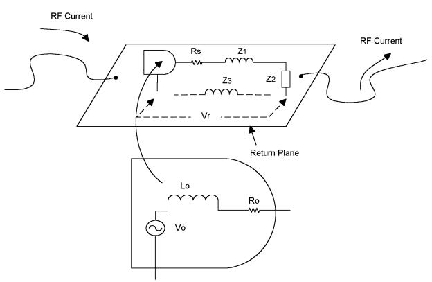
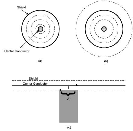
Figure 2: The return plane has a
partial inductance and therefore will exhibit a voltage drop Vr across it. This voltage drop causes wires connected to
the return to radiate.
The concept of partial inductance is useful for solving
problems that would otherwise seem intractable. Take, for example, the calculation of the inductance of a single
straight, infinitely long wire. In
theory, only loops have inductance.
Nonetheless, we have all experienced situations where a wire seems to
have an inductance per unit length even where the current loop seems impossible
to define. Using the concept of partial
inductance, however, we calculate the drop expected per unit length of wire due
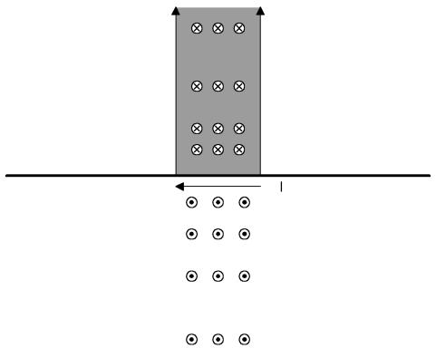
to inductance (Figure 3). The flux
through the area shown in Figure 3 -- which is defined as a surface of infinite
length perpendicular to a selected segment of the wire -- divided by the
current in that segment yields the partial inductance.

Figure 3: The partial inductance of a straight segment
of wire can be calculated by taking the flux through the shaded area and
dividing it by the current.
So far we have been talking
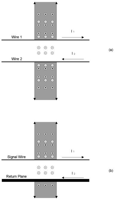
about the inductance of a single wire isolated in space. Wires however, are rarely so isolated. Take, for example, the two parallel wires
shown in Figure 4. Here, the partial
inductance of a segment is due both to the flux generated by the current
flowing in wire 1 and the flux generated by the current flowing in wire 2.

Where:
Lp
tot= “Total” partial inductance of a segment of wire 1.
L11
= Partial inductance of wire 1 due to the flux generated by the current on wire
1.
L12
= Partial inductance of wire 1 due to the flux generated by the current on wire
2.

Figure 4: A pair of wires (a)
carrying opposing currents will produce opposing fields in the shaded
areas. Taking the net flux through the
shaded area above wire 1 and dividing by the current on wire 1 allows us to
compute the “total” partial inductance of that segment of wire 1. In the same manner, the partial inductance
of a segment of a return plane can be calculated by taking the flux through the
shaded area below the plane as in (b) and dividing by the current passing
through the plane.
L11 is known as
the self partial inductance. The
term L12 is known as the mutual partial inductance. The total
partial inductance of a segment, Lp tot, is the sum of the self
and mutual inductances. Lp tot is sometimes known as the effective
inductance, L eff.
The sign on the right side of
this equation is a function of the direction of the current in wire 2. If the current in wire 2 flows in the same
direction as the current in wire 1 then the equation becomes:

The effect of wire 2 is then
to raise the inductance of wire 1.
For symmetrical structures
such as the two wires of Figure 4(a), the calculation of partial inductance is
straightforward. For structures that
are not symmetrical, however, such as the classic case of a wire over a plane
(Figure 4(b)), the calculations become considerably more complex. Nonetheless, some important insight can be
gained by keeping these things in mind:
1. The total
inductance of any loop can, by definition, be calculated by taking the flux
through a surface bounded by the loop and dividing it by the current.
2. The partial
inductance of a segment of a signal wire (Figure 4(b)) can be calculated by
mapping a rectangular area outside the loop formed by the signal wire
and the plane as shown. Calculating the
flux in this area and dividing by the current yields the partial inductance of
that segment.
3. The partial
inductance of a segment of the return plane is calculated by identifying a
rectangular area beneath the return plane and calculating the flux
through it. That flux divided by the
current yields the partial inductance of that segment of the plane.
The larger the return plane’s
partial inductance, the greater the radiation that is likely to result. Consider the case of a digital clock driving
a load (Figure 2). Any inductance in
the return plane will cause a voltage drop across it. That voltage will cause wires attached to the return plane to
radiate like an antenna. Neglecting
resistances, the voltage drop is equal to:

Where:
Vr
= Voltage dropped across the return plane
w = Frequency
in radians per second = 2pf
Lp
= Partial inductance of the return plane
Ir = Current through the return plane
Controlling the partial
inductance of the return plane is therefore of great importance in controlling
emissions. Making the return plane
infinitely wide will result in a return plane partial inductance of zero. An infinitely wide return plane will prevent
any lines of magnetic flux from passing through it .
Note that the same logic
applies to the case of the ideal shielded cable (Figure 5(a)). Here, all the lines of flux created by the
center conductor are trapped within the shield. No lines of flux extend beyond the shield and therefore the
partial inductance of the shield is zero.
The center conductor, through the sum of its partial inductances,
represents all the inductance of a circuit formed by the center conductor and
the shield.

Figure 5: An ideal shielded
cable (a) exhibits no return inductance.
However, all practical shielded cables have some flux leakage (b). The flux around the shield causes it to
exhibit an inductance and a voltage drop as shown in (c). This voltage drop can cause the shield to
radiate.

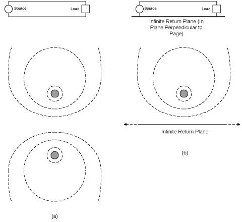
Figure 6: An open wire
transmission line produces a classical dipole like magnetic flux pattern as
shown in (a). The pattern produced by a
wire over an infinite return plane (b) is the same (at least above the plane).

Figure 7: Real return planes are finite in size, so
some flux leaks around the edges of the return plane, accounting for its
partial inductance.
In the case of a shielded
cable, any flux that is lost (that is, which circulates around the shield
rather than within it) accounts for partial inductance of the shield and will
result in a voltage drop across a portion of the shield. That voltage will drive the rest of the
cable, and devices attached to it, as if they were antennas. The same concept of “lost flux” can be
applied to the case of a wire over a plane.
Flux that wraps around the plane is essentially lost and minimizing this
lost flux is a key to minimizing the voltage drop across the plane (Figure 7).
In a 1995 paper (Ref. 2)
Leferink tabulated the predicted partial inductances of the return conductors
in various circuits (Figures 8 and 9 and Table 1). To make things manageable, Leferink had to make a number of
assumptions. These were:
1. All of
the marked dimensions In Figures 8 and 9 are considered to be small compared to
the wavelength of interest.
2. The
current distribution in the signal conductor (or to use Leferink’s terminology,
the Flux Generating Conductor, FGC) is considered to be uniform.
3. The
length of any transmission line formed is much greater than all the other
dimensions.
4. The
radius r where shown or the thickness t are considered to be
equal for the signal conductor and the return conductor.

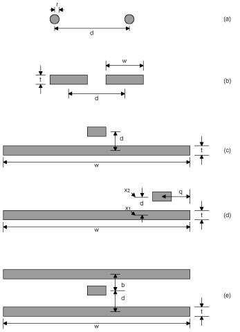
Figure 8: Some common geometries. The return partial inductance is tabulated
for each in Table 1.

Figure 9: Gaps (a) and holes (c) can raise the return
plane’s impedance. Figure 9(b) is a side view of the arrangement.
The formulas allow us to
predict, to at least a first approximation, the partial inductance associated
with some common geometries. Take, for
example, a trace suspended above a plane (Figure 8c). The formulas predict that the effective inductance falls as the
width of the plane is incresed. We also
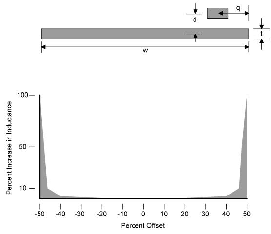
can calculate the effect of moving a signal conductor closer to the edge of a
plane (Figure 8d). Here the formulas
predict that the inductance of the return plane will rise as the signal
conductor gets closer to the edge of the plane. However, this rise is small until the signal conductor gets quite
close to the edge (Figure 10).

Figure 10: Moving a trace
towards the edge of a return plane raises its inductance.
Finally, we can use the
formulas to predict the increase in a return plane’s inductance due to holes or
a gap in the return plane. For a gap
whose dimensions are l=10mm, g=50mm and t=0.035mm, Lgap=14.5nH. For a plane studded with holes of r=1mm
and d=1.6mm, each hole over which the signal wire passes will contribute
17 pH. Small holes in the return plane
do not tend to increase inductance markedly, though gaps do.
References
- T. Hubing, T. Van Doren and J. Drewniak,
“Identifying and Quantifying Printed Circuit Board Inductance,” IEEE
Symposium on Electromagnetic Compatibility, 1994, Page 205.
- F. Leferink, “Inductance Calculations; Methods
and Equations,” IEEE Symposium on Electromagnetic Compatibility, 1995,
Page 16.
- F. Leferink, “Preventing Electromagnetic
Interference from Integrated Circuits and Printed Circuit Boards using
Computer Simulation,” Twente University of Technology, Rep. EL-BSC-92N138,
1992.
- F. Buesink, “Inductance of Striplines,” Internal
Note to F. Leferink, Hollandse Signaalapparaten B. V.
- H. Kaden, Wirbelstroeme und Schirmung in der
Nachrichtentechnik, Springer, Berlin, 1959.
- F. Leferink, M. van Doorn, “Inductance of Printed
Circuit Board Ground Planes,” IEEE Symposium on Electromagnetic
Compatibility, 1993, Page 327.
- D. Hockanson, J. Drewniak, T. Hubing, T. Van
Doren, F. Shu, C. Lam, L. Rubin, “Quantifying EMI Resulting from
Finite-Impedance Reference Planes,” IEEE Transactions on Electromagnetic
Compatibility, Nov. 1997, Page 286.
TABLE 1
After Leferink (Reference 2)
|
Description of Circuit
|
Figure
|
Leff—Partial Inductance of Return
|
Notes
|
|
Ideal Shielded Cable
|
5(a)
|
0
|
Ideal Case
|
|
Open Wire Transmission Line
|
8(a)
|

|
Radii equal
|
|
Traces Side by Side
|
8(b)
|

|
Edge effects ignored
|
|
Microstrip
|
8(c)
|

|
After Leferink (Ref. 6)
|
|
Microstrip
|
8(c)
|

|
After Hockanson (Ref. 7)
|
|
Offset Microstrip
|
8(d)
|

|
|
|
Stripline
|
8(e)
|

|
After Buesink. (Ref. 4)
t=0
|
|
Return Plane with Gap
|
9(a), 9(b)
|

|
g>d
|
|
Return Plane with Holes
|
9(b), 9(c)
|

|
After Kaden (Ref. 5)
v = holes per unit length
|
Note: l in the equations above is the length of
the return or a portion of the return.
It does not appear in Figure 8.
Inductances are in Henries. In
terms of inductance per unit length, the term (m/2p)=2nH/cm.
![]()
